In this tutorial, we will learn How to Use ADC with our PIC microcontroller PICF877A. Most of the Microcontroller projects will involve an ADC (Analog to Digital converter) in it, because it is one the most used ways to read data from the real world. Almost all the sensors like temperature sensor, flux sensor, pressure sensor, current sensors, voltage sensors, gyroscopes, accelerometers, distance sensor, and almost every known sensor or transducer produces an analog voltage of 0V to 5V based on the sensors reading. A temperature sensor for instance may give out 2.1V when the temperature is 25C and go upto 4.7 when the temperature is 60C. In order to know the temperature of the real world, the MCU has to just read the output voltage of this temperature sensor and relate it to the real world temperature. Hence ADC is an important work tool for MCU projects and lets learn how we can use it on our PIC16F877A.
ADC in PIC Microcontroller PIC16F877A:
There are many types of ADC available and each one has its own speed and resolution. The most common types of ADCs are flash, successive approximation, and sigma-delta. The type of ADC used in PIC16F877A is called as the Successive approximation ADC or SAR in short. So let’s learn a bit about SAR ADC before we start using it.
Successive Approximation ADC: The SAR ADC works with the help of a comparator and some logic conversations. This type of ADC uses a reference voltage (which is variable) and compares the input voltage with the reference voltage using a comparator and difference, which will be a digital output, is saved from the Most significant bit (MSB). The speed of the comparison depends on the Clock frequency (Fosc) on which the PIC is operating.
Now that we know some basics on ADC, lets open our datasheet and learn how to use the ADC on our PIC16F877A MCU. The PIC we are using has 10-bit 8-channel ADC. This means the output value of our ADC will be 0-1024 (2^10) and there are 8 pins (channels) on our MCU which can read analog voltage. The value 1024 is obtained by 2^10 since our ADC is 10 bit. The eight pins which can read the analog voltage are mentioned in the datasheet. Lets look at the picture below.
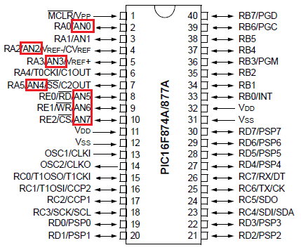
The analog channels AN0 to AN7 are highlighted for you. Only these pins will be able to read analog voltage. So before reading an input voltage we have to specify in our code which channel has to be used to read the input voltage. In this tutorial we will use channel 4 with a potentiometer to read the analog voltage at this channel.
The A/D module has four registers which has to be configured to read data from the Input pins. These registers are:
• A/D Result High Register (ADRESH)
• A/D Result Low Register (ADRESL)
• A/D Control Register 0 (ADCON0)
• A/D Control Register 1 (ADCON1)
Programming for ADC:
The program for using ADC with PIC Microcontroller is very simple, we just have to understand these four registers and then reading any analog voltage will be simple. As usual initialize the configuration bits and let’s start with the void main().
Inside the void main() we have to initialize our ADC by using the ADCON1 register and ADCON0 register. The ADCON0 register has the following bits:
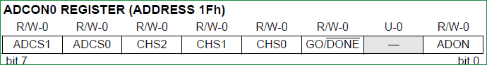
In this register we have to turn on the ADC module by making ADON=1 and turn on the A/D Conversion Clock by using the bits ADCS1 and ADCS0 bits, the rest will not be set for now. In our program the A/D conversion clock is selected as Fosc/16 you can try your own frequencies and see how the result changes. Complete details available on datasheet’s page 127. Hence ADCON0 will be initialised as follows.
ADCON0 = 0b01000001;
Now the ADCON1 register has the following bits:
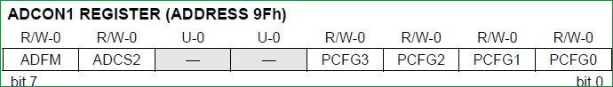
In this register we have to make A/D Result Format Select bit high by ADFM=1 and make ADCS2 =1 to select the Fosc/16 again. The other bits remain zero as we have planned to use the internal reference voltage. Complete details available on datasheet page 128. Hence ADCON1 will we set as follows.
ADCON1 = 0x11000000;
Now after initializing the ADC module inside our main function, lets get into the while loop and start reading the ADC values. To read an ADC value the following steps has to be followed.
- Initialize the ADC Module
- Select the analog channel
- Start ADC by making Go/Done bit high
- Wait for the Go/DONE bit to get low
- Get the ADC result from ADRESH and ADRESL register
1. Initialize the ADC Module: We have already learnt how to initialize an ADC so we just call this below function to initialize the ADC
The void ADC_Initialize() function is be as follows.
void ADC_Initialize()
{
  ADCON0 = 0b01000001; //ADC ON and Fosc/16 is selected
  ADCON1 = 0b11000000; // Internal reference voltage is selected
}
2. Select the analog channel: Now we have to select which channel we are going to use to read the ADC value. Lets make a function for this, so that it will be easy for us to shift between each channel inside the while loop.
unsigned int ADC_Read(unsigned char channel)
{
    //****Selecting the channel**///
  ADCON0 &= 0x11000101; //Clearing the Channel Selection Bits
  ADCON0 |= channel<<3; //Setting the required Bits
  //**Channel selection complete***///
}
Then channel to be selected is received inside the variable channel. In the line
ADCON0 &= 0x1100101;
The previous channel selection (if any) is cleared. This is done by using the bitwise and operator “&”. The bits 3, 4 and 5 are forced to be 0 while the others are left to be in their previous values.
Then the desired channel is selected by left shifting the channel number thrice and setting the bits using the bitwise or operator “|”.
ADCON0 |= channel<<3; //Setting the required Bits
3. Start ADC by making Go/Done bit high: Once the channel is selected we have to start the ADC conversion simply by making the GO_nDONE bit high:
GO_nDONE = 1; //Initializes A/D Conversion
4. Wait for the Go/DONE bit to get low: The GO/DONE bit will stay high until the ADC conversion has been completed, hence we have to wait till this bit goes low again. This can be done by using a whileloop.
while(GO_nDONE); //Wait for A/D Conversion to complete
Note: Placing a semi-colon next to while will make the program to be held there till the condtion of the while loop is false.
5. Get the ADC result from ADRESH and ADRESL register: When the Go/DONE bit gets low again it means that the ADC conversion is complete. The result of the ADC will be a 10-bit value. Since our MCU is a 8-bit MCU the result is split into upper 8-bit and the lower 2-bits. The upper 8-bit result is stored in the register ADRESH and the lower 2-bit is stored in the register ADRESL. Hence we have to add up these to registers to get our 10-bit ADC value. This result is returned by the function as shown below:
return ((ADRESH<<8)+ADRESL); //Returns Result
The complete function which is used to select the ADC channel, trigger the ADC and return the result is shown here.
unsigned int ADC_Read(unsigned char channel)
{
  ADCON0 &= 0x11000101; //Clearing the Channel Selection Bits
  ADCON0 |= channel<<3; //Setting the required Bits
  __delay_ms(2); //Acquisition time to charge hold capacitor
  GO_nDONE = 1; //Initializes A/D Conversion
  while(GO_nDONE); //Wait for A/D Conversion to complete
  return ((ADRESH<<8)+ADRESL); //Returns Result
}
Now we have a function which will take the channel selection as input and return us the ADC value. Hence we can directly call this function inside our while loop, since we are reading the analog voltage from channel 4 in this tutorial, the function call will be as follows.
i = (ADC_Read(4)); //store the result of adc in “i”.
In order to visualize the output of our ADC we will be needing some sort of display modules like the LCD or the 7-segment.
The complete code is given below and the process is also explained in the Video at the end.
Hardware Setup and Testing:
As usual simulate the code using Proteus before actually go with our hardware, the schematics of the project is shown below:

Connections of 4-digit seven segment display module with PIC microcontroller are same as the previous project, we have just added a potentiometer to the pin 7 which is the analog channel 4. By varying the pot, a variable voltage will be sent to the MCU which will be read by the ADC module and displayed on the 7-segment display Module.
Here we have used the same PIC Microcontroller board which we have created in LED blinking Tutorial. After ensuring connection upload the program into PIC and you should see an output like this
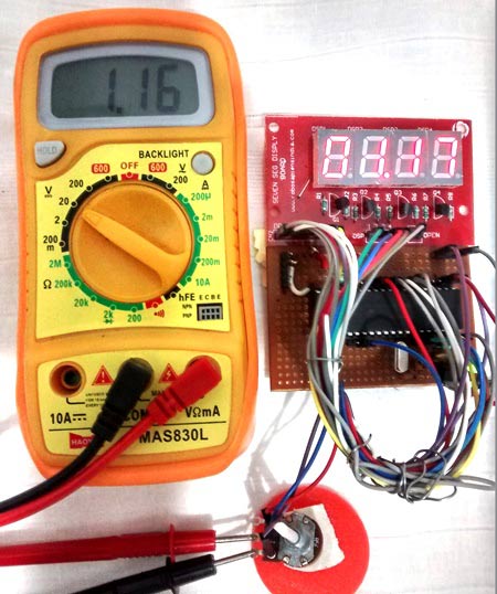
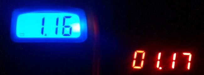
Here we have read the ADC value from the pot and converted it to the actual voltage by mapping the 0-1024 output as 0-5 volts (as shown in program). The value is then displayed on the 7-segment and verified using the multimeter.
Thats it, now we are ready to use all the Analog Sensors available in the market, go ahead and try this and if you have any problems as usual use the comment section, we will be happy to help you out.
Code:
// CONFIG
#pragma config FOSC = HS // Oscillator Selection bits (HS oscillator)
#pragma config WDTE = OFF // Watchdog Timer Enable bit (WDT disabled)
#pragma config PWRTE = ON // Power-up Timer Enable bit (PWRT enabled)
#pragma config BOREN = ON // Brown-out Reset Enable bit (BOR enabled)
#pragma config LVP = OFF // Low-Voltage (Single-Supply) In-Circuit Serial Programming Enable bit (RB3 is digital I/O, HV on MCLR must be used for programming)
#pragma config CPD = OFF // Data EEPROM Memory Code Protection bit (Data EEPROM code protection off)
#pragma config WRT = OFF // Flash Program Memory Write Enable bits (Write protection off; all program memory may be written to by EECON control)
#pragma config CP = OFF // Flash Program Memory Code Protection bit (Code protection off)
// #pragma config statements should precede project file includes.
// Use project enums instead of #define for ON and OFF.
// Use project enums instead of #define for ON and OFF.
#include <xc.h>
#define _XTAL_FREQ 20000000
#define _XTAL_FREQ 20000000
//***Define the signal pins of all four displays***//
#define s1 RC0
#define s2 RC1
#define s3 RC2
#define s4 RC3
//***End of definition**////
#define s1 RC0
#define s2 RC1
#define s3 RC2
#define s4 RC3
//***End of definition**////
void ADC_Initialize()
{
ADCON0 = 0b01000001; //ADC ON and Fosc/16 is selected
ADCON1 = 0b11000000; // Internal reference voltage is selected
}
{
ADCON0 = 0b01000001; //ADC ON and Fosc/16 is selected
ADCON1 = 0b11000000; // Internal reference voltage is selected
}
unsigned int ADC_Read(unsigned char channel)
{
ADCON0 &= 0x11000101; //Clearing the Channel Selection Bits
ADCON0 |= channel<<3; //Setting the required Bits
__delay_ms(2); //Acquisition time to charge hold capacitor
GO_nDONE = 1; //Initializes A/D Conversion
while(GO_nDONE); //Wait for A/D Conversion to complete
return ((ADRESH<<8)+ADRESL); //Returns Result
}
void main()
{ int a,b,c,d,e,f,g,h,adc; //just variables
int i = 0; //the 4-digit value that is to be displayed
int flag =0; //for creating delay
{ int a,b,c,d,e,f,g,h,adc; //just variables
int i = 0; //the 4-digit value that is to be displayed
int flag =0; //for creating delay
unsigned int seg[]={0X3F, //Hex value to display the number 0
0X06, //Hex value to display the number 1
0X5B, //Hex value to display the number 2
0X4F, //Hex value to display the number 3
0X66, //Hex value to display the number 4
0X6D, //Hex value to display the number 5
0X7C, //Hex value to display the number 6
0X07, //Hex value to display the number 7
0X7F, //Hex value to display the number 8
0X6F //Hex value to display the number 9
}; //End of Array for displaying numbers from 0 to 9
//*****I/O Configuration****//
TRISC=0X00;
PORTC=0X00;
TRISD=0x00;
PORTD=0X00;
//***End of I/O configuration**///
TRISC=0X00;
PORTC=0X00;
TRISD=0x00;
PORTD=0X00;
//***End of I/O configuration**///
ADC_Initialize();
#define _XTAL_FREQ 20000000
while(1)
{
if(flag>=50) //wait till flag reaches 100
{
adc = (ADC_Read(4));
i = adc*0.488281;
flag=0; //only if flag is hundred "i" will get the ADC value
}
flag++; //increment flag for each flash
{
if(flag>=50) //wait till flag reaches 100
{
adc = (ADC_Read(4));
i = adc*0.488281;
flag=0; //only if flag is hundred "i" will get the ADC value
}
flag++; //increment flag for each flash
//***Splitting "i" into four digits***//
a=i%10;//4th digit is saved here
b=i/10;
c=b%10;//3rd digit is saved here
d=b/10;
e=d%10; //2nd digit is saved here
f=d/10;
g=f%10; //1st digit is saved here
h=f/10;
//***End of splitting***//
a=i%10;//4th digit is saved here
b=i/10;
c=b%10;//3rd digit is saved here
d=b/10;
e=d%10; //2nd digit is saved here
f=d/10;
g=f%10; //1st digit is saved here
h=f/10;
//***End of splitting***//
PORTD=seg[g];s1=1; //Turn ON display 1 and print 4th digit
__delay_ms(5);s1=0; //Turn OFF display 1 after 5ms delay
PORTD=seg[e];RD7=1;s2=1; //Turn ON display 2 and print 3rd digit
__delay_ms(5);s2=0; //Turn OFF display 2 after 5ms delay
PORTD=seg[c];s3=1; //Turn ON display 3 and print 2nd digit
__delay_ms(5);s3=0; //Turn OFF display 3 after 5ms delay
PORTD=seg[a];s4=1; //Turn ON display 4 and print 1st digit
__delay_ms(5);s4=0; //Turn OFF display 4 after 5ms delay
}
}
No comments:
Post a Comment