In this tutorial, we will learn How to generate PWM signals using PIC PIC16F877A. Our PIC MCU has a special module called Compare Capture module (CCP) which can be used to generate PWM signals. Here, we will generate a PWM of 5 kHz with a variable duty cycle from 0% to 100%. To vary the duty cycle we are using a potentiometer, hence it is recommended to learn ADC tutorial before starting with PWM. PWM module also uses timers to set its frequency hence learn how to use timers beforehand here. Further, in this tutorial we will use a RC circuit and a LED to convert the PWM values to Analog voltage and use it for dimming the LED light.
What is a PWM Signal?
Pulse Width Modulation (PWM) is a digital signal which is most commonly used in control circuitry. This signal is set high (5v) and low (0v) in a predefined time and speed. The time during which the signal stays high is called the “on time” and the time during which the signal stays low is called the “off time”. There are two important parameters for a PWM as discussed below:
Duty cycle of the PWM:
The percentage of time in which the PWM signal remains HIGH (on time) is called as duty cycle. If the signal is always ON it is in 100% duty cycle and if it is always off it is 0% duty cycle.
Duty Cycle =Turn ON time/ (Turn ON time + Turn OFF time)
Frequency of a PWM:
The frequency of a PWM signal determines how fast a PWM completes one period. One Period is complete ON and OFF of a PWM signal as shown in the above figure. In our tutorial we will set a frequency of 5KHz.
PWM using PIC16F877A:
PWM signals can be generated in our PIC Microcontroller by using the CCP (Compare Capture PWM) module. The resolution of our PWM signal is 10-bit, that is for a value of 0 there will be a duty cycle of 0% and for a value of 1024 (2^10) there be a duty cycle of 100%. There are two CCP modules in our PIC MCU (CCP1 And CCP2), this means we can generate two PWM signals on two different pins (pin 17 and 16) simultaneously, in our tutorial we are using CCP1 to generate PWM signals on pin 17.
The following registers are used to generate PWM signals using our PIC MCU:
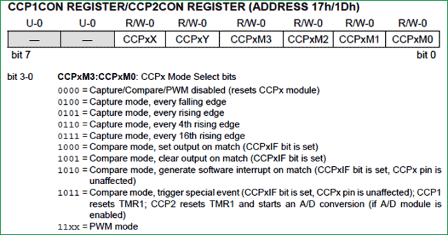
- CCP1CON (CCP1 control Register)
- T2CON (Timer 2 Control Register)
- PR2 (Timer 2 modules Period Register)
- CCPR1L (CCP Register 1 Low)
Programming PIC to generate PWM signals:
In our program we will read an Analog voltage of 0-5v from a potentiometer and map it to 0-1024 using our ADC module. Then we generate a PWM signal with frequency 5000Hz and vary its duty cycle based on the input Analog voltage. That is 0-1024 will be converted to 0%-100% Duty cycle. This tutorial assumes that you have already learnt to use ADC in PIC if not, read it from here, because we will skip details about it in this tutorial.
So, once the configuration bits are set and program is written to read an Analog value, we can proceed with PWM.
The following steps should be taken when configuring the CCP module for PWM operation:
- Set the PWM period by writing to the PR2 register.
- Set the PWM duty cycle by writing to the CCPR1L register and CCP1CON<5:4> bits.
- Make the CCP1 pin an output by clearing the TRISC<2> bit.
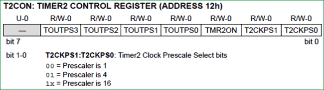
- Set the TMR2 prescale value and enable Timer2 by writing to T2CON.
- Configure the CCP1 module for PWM operation.
There are two important functions in this program to generate PWM signals. One is the PWM_Initialize() function which will initialize the registers required to set up PWM module and then set the frequency at which the PWM should operate, the other function is the PWM_Duty() function which will set the duty cycle of the PWM signal in the required registers.
PWM_Initialize()
{
  PR2 = (_XTAL_FREQ/(PWM_freq*4*TMR2PRESCALE)) - 1; //Setting the PR2 formulae using Datasheet // Makes the PWM work in 5KHZ
    CCP1M3 = 1; CCP1M2 = 1;  //Configure the CCP1 module
    T2CKPS0 = 1;T2CKPS1 = 0; TMR2ON = 1; //Configure the Timer module
    TRISC2 = 0; // make port pin on C as output
}
The above function is the PWM initialize function, in this function The CCP1 module is set to use PWM by making the bit CCP1M3 and CCP1M2 as high.
The timer module’s prescaler is set by making the bit T2CKPS0 as high and T2CKPS1 as low the bit TMR2ON is set to start the timer.
Now, we have to set the Frequency of the PWM signal. The value of the frequency has to be written to the PR2 register. The desired frequency can be set by using the below formulae
PWM Period = [(PR2) + 1] * 4 * TOSC * (TMR2 Prescale Value)
Rearranging these formulae to get PR2 will give
PR2 = (Period / (4 * Tosc * TMR2 Prescale )) - 1
We know that Period = (1/PWM_freq) and Tosc = (1/_XTAL_FREQ). Therefore.....
PR2 = (_XTAL_FREQ/ (PWM_freq*4*TMR2PRESCALE)) – 1;
Once the frequency is set this function need not be called again unless and until we need to change the frequency again. In our tutorial I have assigned PWM_freq = 5000; so that we can get a 5 KHz operating frequency for our PWM signal.
Now let us set the duty cycle of the PWM by using the below function
PWM_Duty(unsigned int duty)
{
      if(duty<1023)
  {

    duty = ((float)duty/1023)*(_XTAL_FREQ/(PWM_freq*TMR2PRESCALE)); // On reducing //duty = (((float)duty/1023)*(1/PWM_freq)) / ((1/_XTAL_FREQ) * TMR2PRESCALE);
    CCP1X = duty & 1; //Store the 1st bit
    CCP1Y = duty & 2; //Store the 0th bit
    CCPR1L = duty>>2;// Store the remining 8 bit
  }
}
Our PWM signal has 10-bit resolution hence this value cannot be stored in a single register since our PIC has only 8-bit data lines. So we have use to other two bits of CCP1CON<5:4> (CCP1X and CCP1Y) to store the last two LSB and then store the remaining 8 bits in the CCPR1L Register.
The PWM duty cycle time can be calculated by using the below formulae:
PWM Duty Cycle = (CCPRIL:CCP1CON<5:4>) * Tosc * (TMR2 Prescale Value)
Rearranging these formulae to get value of CCPR1L and CCP1CON will give:
CCPRIL:CCP1Con<5:4> = PWM Duty Cycle / (Tosc * TMR2 Prescale Value)
The value of our ADC will be 0-1024 we need that to be in 0%-100% hence, PWM Duty Cycle = duty/1023. Further to convert this duty cycle into a period of time we have to multiply it with the period (1/ PWM_freq)
We also know that Tosc = (1/PWM_freq), hence..
Duty = ( ( (float)duty/1023) * (1/PWM_freq) ) / ( (1/_XTAL_FREQ) * TMR2PRESCALE) ;
Resolving the above equation will give us:
Duty = ( (float)duty/1023) * (_XTAL_FREQ / (PWM_freq*TMR2PRESCALE));
You can check the complete program in the Code section below along with the detailed Video.
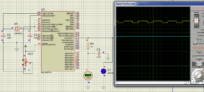
Schematics and Testing:
As usual let us verify the output using Proteus simulation. The Circuit Diagram is shown below.
Connect a potentiometer to 7th pin to feed in a voltage of 0-5. CCP1 module is with pin 17 (RC2), here the PWM will be generated which can be verified using the Digital oscilloscope. Further to convert this into a variable voltage we have used a RC-filter and an LED to verify the output without a scope.
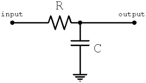
What is a RC-Filter?
An RC filter or a Low pass filter is a simple circuit with two passive elements namely the resistor and the capacitor. These two components are used to filter the frequency of our PWM signal and make it a variable DC voltage.
If we examine the circuit, when a variable voltage is applied to the input of R, the capacitor C will begin to charge. Now based on the value of the capacitor, the capacitor will take some time to get fully charged, once charged it will block the DC current (Remember capacitors block DC but allows AC) hence the input DC voltage will appear across the output. The high frequency PWM (AC signal) will be grounded through the capacitor. Thus a pure DC is obtained across the capacitor. A value of 1000Ohm and 1uf was found to be appropriate for this project. Calculating the values of R and C involves circuit analysis using transfer function, which is out of scope of this tutorial.

The output of the program can be verified using the Digital Oscilloscope as shown below, vary the Potentiometer and the Duty cycle of the PWM should change. We can also notice the output voltage of the RC circuit using the Voltmeter. If everything is working as expected we can proceed with our hardware. Further check the Video at the end for full process.
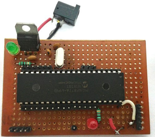
Working on Hardware:
The hardware setup of the project is very simple, we are just going to reuse our PIC perf boards shown below.
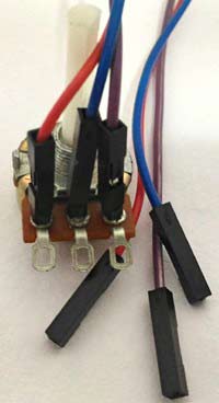
We will also need a potentiometer to feed in the analog voltage, I have attached some female end wires to my pot (shown below) so that we can directly connect them to the PIC Perf board.
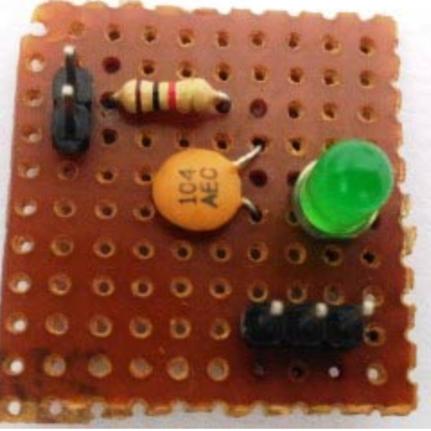
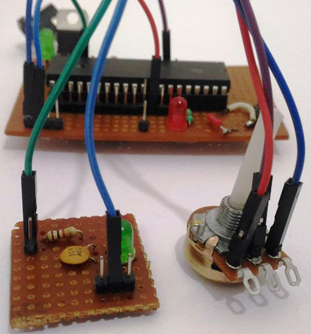
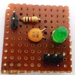
Finally to verify the output we need a RC circuit and a LED to see how the PWM signal works, I have simply used a small perf board and soldered the RC circuit and the LED (to control brightness) on to it as shown below
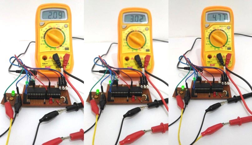
We can use simple female to female connecting wires and connect them according to the schematics shown above. Once the connection is done, upload the program to the PIC using our pickit3 and you should be able to get a variable voltage based on the input of your potentiometer. The variable output is used to control the brightness of the LED here.
I used my multimeter to measure the variable outputs, we can also notice the brightness of the LED getting changed for different voltage levels.
That’s it we have programmed to read the Analog voltage from the POT and convert into PWM signals which in turn have been converted into Variable voltage using RC filter and the result is verified using our hardware. If you have some doubt or get stuck somewhere kindly use the comment section below, we will be happy to help you out. The complete working is working in the video.


 In conventional voltage multiplier circuits, AC is used to charge the capacitors network via diodes in one cycle and discharge in the other cycle in a particular combination, which thereby produces multiples of the peak voltage. However, this circuit works on a different principle, and it is DC which is doubled. It can be used to power low current circuits.