Tuesday, September 20, 2022

How many KVA makes 3300 watts?

We can easily calculate it by using our Power Triangle Formula. It is the most authentic method of calculating the Watts from KVA or vice versa.

Where;

S = Apparent Power = KVA
P = Actual Power or Real Power = KW
Q = Reactive Power = KVAR

If we have Power factor known, then it is very easy to determine the other values. If p.f is not known, we assume the power factor to be 0.8 or 0.9 for an equipment or a system.

Let’s say we have a generator of 10 KVA, with a p.f of 0.8 lagging, then we can easily calculate the KW in this way.

p.f = KW/KVA

Just plug in the values.

0.8 = KW/10

KW = 10*0.8

KW =8

SO WE GET A POWER OF 8000 WATTS


In your case, lets assume,we have p.f of 0.8 and 3300 watts, so calculate KVA’s in this way;

p.f = KW/KVA

0.8 = 3.3/KVA

OR

KVA = 3.3/0.8

KVA = 4.125

Or;

4.125 kVA MAKES 3300 WATTS.

Sunday, September 18, 2022

intruder alarm

Intruder Alarm


  Intruder alarm is very common project for diploma or basic level. Here, by dreamlover technology a verified project on intruder is published, used in door of your house for sound an alarm when anyone open or pushed the door. The circuit of intruder alarm can be used against thieves or intruders.

  The project intruder alarm consist two circuits each of transmitter and receiver separately. Transmitter section comprising a laser diode and power is given from a 9V power supply. Here the receiving section consists of LDR for sensor and work on principle of LDR. When light falling to LDR from laser diode provides base current to transistor T1 which start conducting (but not T2) and the alarm remains off.

  When door is pushed, light incident on the LDR is interrupted and it offer high resistance which stop conducting transistor T1 but transistor T2 receive base current and start conducting. The input is given to AND gate N1 from the emitter of transistor T2. Here IC2 work as latch when high output from AND gate N1 is connected to pin 1 and 14 respectively. High output form output pin 12 of IC2 is given to base of transistor T3 through R7 and it cause transistor conduction and consequent sounding of the alarm.

Parts List

Resistors (all ¼-watt, ± 5% Carbon)

R1, R2, R6, R8 = 1 KΩ

R3 = 2.2 KΩ

R4 = 10 KΩ

R5 = 100 Ω

R7 = 2.2 KΩ

Semiconductors

IC1 (N1) = 7408

IC2 = 7473 JK Flip-Flop

T1 = BEL187

T2, T3 = SL100

LED1, LED2 = RED

LD1 = Laser Diode

Miscellaneous

9V Battery

SW1, SW2 = On/Off Switch

SW3 = Push-to-On Switch

Piezo Buzzer

LDR

traffic light control

Traffic Light Controller


  The circuit given here is substitute of old mechanical traffic-light controllers which are not reliable. The circuit’s timing and sequential operation are done by two CMOS ICs (IC1 and IC2) while the actual power switching is done by triacs,

  A 10V negative power supply is obtained directly from the mains my means of D1, R1, D2, and C1. Gates N1 through N6 constitute IC2 while IC1 is a Johnson counter. N1 – N3 are wired as an astable multivibrator whose time period can be adjusted between 1 second and 10 seconds with VR1. The decade outputs of IC1 are wired such that when Q0 and Q5 is high, the output of N5 goes low. Similarly, the outputs of N4 and N6 become low when Q1 to Q4 and Q6 to Q9 become low respectively. Since we have negative supply, a low output of any of the hates N4 to N6 cause the respective triac to fire.

  Thus, the ratios of the time periods for the lamps in the sequence O:G:O:R are 1:4:1:4.

  Resistor R10 to R12 and capacitor C4 and C6 are absolutely necessary, these avoid spurious triggering of the triacs which may hamper traffic flow.

Parts List

Resistors (all ¼-watt, ± 5% Carbon unless stated otherwise)

R1 = 5 KΩ/5W
R2, R3, R4 = 22 KΩ
R5 = 100 KΩ
R6 = 1 MΩ
R7, R8, R9 = 1 KΩ
R10, R11, R12 = 100 Ω/1W
VR1 = 1 MΩ

Capacitors

C1 = 1000 µF/16V
C2, C3 = 22 µF/16V
C4, C5, C6 = 00.1 µF/400V

Semiconductors

IC1 = CD4017
IC2(N1 – N6) = CD4049
D1 = BY127

universal battery tester

Universal Battery Tester


  To recognize the battery whether it is working or not is very difficult. Generally voltmeter is employed for checking purpose of state of battery. Now, here is very simple circuit utilized to check the state of battery.

  The entire circuit of universal battery tester is build around dual comparator IC TL072 (IC1) followed by other component. The two independent comparator is used here as operational amplifier. The inverting pin of these two operational amplifiers is fed through potential divider network made from resistor R1 and R3. Rest of the component is utilized to maintain threshold voltage.

  State of LED
  Glowing RED LED:- Battery is fully charged
  Glowing GREEN LED:- Battery is usable
  Glowing RED LED:- Need charge or it is not usable.

Parts List

Resistors (all ¼-watt, ± 5% Carbon unless stated otherwise)

R1, R3 = 5.6 Ω
R2 = 3.3 KΩ
R4, R6 = 1 MΩ
R5, R7, R9 = 1 KΩ
R8, R10 = 820 Ω
R11 = 10 KΩ

Semiconductors

IC1 = TL072CD
ZD1 = 3.3 V/500mW
LED1 = RED LED
LED2 = GREEN LED
LED3 = YELLOW LED

Miscellaneous

SW1 = Push to on switch
Two probe

simple low/high voltage cut off circuit

Simple Low/High Voltage Cut Circuit


  Various safety circuit (low/high voltage cut) using IC is already published in www.electronicsproject.org. Now, here is very simple low/high voltage cut circuit using only two transistors.

  The entire circuit is build using only two transistor and very few other component. The two transistors are used to drive relay. Transistor T1 and T2 cut the supply in high and low voltage respectively. Variable resistor VR1 and VR2 is used to adjust the high and low voltage. As we know that when zener diode is connected to emitter of transistor then it get back bias voltage. The variable resistor VR1 and VR2 is so adjusted that it does not connect the transistor T2 and T1 in high and low voltage respectively. The load is connected through relay RL1.

Parts List

Resistors (all ¼-watt, ± 5% Carbon unless stated otherwise)

R1, R4 = 4.7 KΩ
R2, R3 = 220 Ω
VR1 = 10 KΩ
VR2 = 10 KΩ

Semiconductors

T1, T2 = BC148
ZD1, ZD2 = 5.6V

Miscellaneous

RL1 = 18V/500Ω

Mini amplifier

Mini Amplifier


  Here is a simple project , mini amplifier built around LM1895 followed by passive components. The output of 10mW to 1W is obtained so, the circuit is called mini amplifier.

  The output from mike or pre-amplifier is fed to pin no.4 through variable resistor VR1 and capacitor C4. Variable resistor VR1 is used to select the intensity of signal. Capacitor C2 and C6 is used to filter and develop the supply, where capacitor C3 and C5 is used to bias the audio frequency. The output of amplifier IC is obtained at pin 1 where resistor R4 and capacitor C8 is used as feedback component. The output is given to loudspeaker through capacitor C7 in order to produce sound.

Parts List

Resistors (all ¼-watt, ± 5% Carbon unless stated otherwise)

R1 = 10 KΩ
R2 = 47Ω
R3 = 220Ω
R4 = 1Ω
VR1 = 50 KΩ

Capacitors

C1 = 470 pF
C2 = 220 µF/10V
C3 = 100 µF/10V
C4 = 0.1 µF
C5 = 10 µF/10V
C6, C7 = 470 µF/10V
C8 = 0.1 µF

Semiconductors

IC1 = LM1895N
Miscellaneous
LS1 = 4Ω/1W speaker

Battery voltage monitor

Battery Voltage Monitor


  All rechargeable battery has their specific level of charging and discharging, they are likely to get damage if the battery voltage exceeds that level. Here is a simple circuit battery voltage monitor used to indicate the state of battery by monitor them.

  The circuit of battery voltage monitor is fabricated and designed around op-amp IC LM709 configured as comparator. Where bi-color LED is used as indicator and indicates three voltage level state of a 12V battery. Resistor R1 with potentiometer VR1 is used as potential driver of voltage monitor circuit.

  When voltage level rise above 13.5 volts, the output from IC1 goes low as a result LED begins to emit RED light. Similarly, when the voltage fall below a preset level (10Volts) the output goes high and the LED start to emit GREEN light. Resistors R3 and R4 is used as current limiter of LED.

  NOTE: Adjust VR1 such that LED begins to emit GREEN light when 10V DC is connected.

Parts List

Resistors (all ¼-watt, ± 5% Carbon)

R1 = 1 KΩ

R2 = 18 KΩ

R3, R4 = 680 Ω

VR1 = 10 KΩ (Potentiometer)

Semiconductors

IC1 = LM709

D1 = 1N4003

Miscellaneous

B1 = 12V Battery

LED = Bi-color LED

Friday, September 16, 2022

infrared remote control switch

Infrared Remote Control Switch


  Now a day, everyone wants to control their appliance wirelessly (i.e. remote control). Here is a simple tested and inexpensive remote control switch utilizing reading available components

  As in all wireless systems Infrared (IR) remote control switch also comprise two major section i.e. transmitter and receiver section.

  Transmitter Section: – The logic of this section is simple and is build around most versatile IC NE555 (IC1), configured as astable multivibrator to produce frequency about 38 KHz. This is so, because IR module receiver used here works in range of 38 KHz frequency. Timing component of infrared remote control switch is resistor R1 and R2 and capacitor C2, determine the range of oscillating. Where, formula of generated frequency (F) from transmitter section IR remote is given by

  F = 1.443 / (R1 + 2R2) C2

  The output frequency from pin 3 of IC1 is fed to base of transistor T1 through resistor R4 and is configured as Darlington pair with transistor T2 in order to drive IR LED and resistor R5 works as current limiter.

  Receiver Section: – Transmitted signal from transmitter is received by infrared (IR) receiver module (TSOP 1738) and is fed to base of PNP transistor T3 through resistor R6 for amplification. Amplified signal is fed to pin 2 of IC2 through coupling capacitor C6. IC2 is configured as monostable multivibrator which is triggered when low pulse from receiver module is given and its output goes high only for 5 second.

  The output from IC2 is given to pin 14 of decade counter IC (IC3) through resistor R12. Here two outputs (pin 2 and 3) is taken from IC3 which alternately go high for every clock pulse. Initially at starting time (when no signal is received) pin 3 goes high and no gate current pulse is received by TRIAC1. But when signal is received pin 2 goes high and activate TRIAC1, which, in turn controls the appliance.

  NOTE: – Glowing LED1, LED2, LED3 and LED4 is used to indicate signal transmission, presence of power supply in receiver section, signal received and appliance off respectively.

Parts List

Resistors (all ¼-watt, ± 5% Carbon)

R1 = 8.2 KΩ

R2 = 15 KΩ

R3, R8, R11, R12, R13, R15 = 1 KΩ

R4, R14 = 470 Ω

R5 = 10 Ω

R6 = 680 Ω

R7 = 5 KΩ

R9 = 10 KΩ

R10 = 220 KΩ

Capacitors

C1 = 100 µF/25V

C2 = 0.001 µF

C3, C8 = 0.01 µF

C4, C9 = 100 µF/16V

C5, C6 = 10 µF/16V

C7 = 22 µF/16V

Semiconductors

IC1, IC2 = NE555

IC3 = CD4017

IC4 = LM7806

TRIAC1 = BT136

T1, T2 = BC547 (NPN)

T3 = BC558 (PNP)

ZD1 = 5.1 V zener diode

IRX1 = TSOP 1738 (IR receiver module)

Miscellaneous

SW1 = push to on / off switch

LED1 = Green

LED2 = RED

LED3 = Yellow

LED4 = white

voltage stepper

Voltage Stepper

  In conventional voltage multiplier circuits, AC is used to charge the capacitors network via diodes in one cycle and discharge in the other cycle in a particular combination, which thereby produces multiples of the peak voltage. However, this circuit works on a different principle, and it is DC which is doubled. It can be used to power low current circuits.

  IC555 is configured as an astable multivibrator producing rectangular pulses of about 10kHz frequency. Its output is made to drive the transistor pair T1 and T2. Transistor T2 being a pnp type, conduct when its base is negative, i.e. when the output of the IC produces a “low”. This charge C4 via diode D1 and ground (collector of T2 is grounded).

  For the next pulse, i.e. when the output of IC is high, T1 conducts but T2 is cut-off, C4 cannot discharge because of diode D1. So the voltage across C4 and input voltage adds up and charge C5 via D2. Voltage across C5 will equal Vcc pulse voltage across capacitor C4 and Diode D1. Hence the operation.

  However, it was found that if current greater then 50 mA and drawn, output voltage, hence regulation, is lost. Any DC voltage between 5V and 18V can be boosted (both voltage being the minimum and maximum range of the IC).

  For better results, increase the value of C4 and C5 to 47 µF/40V.

Parts List

Resistors (all ¼-watt, ± 5% Carbon)

R1 = 220 Ω

R2 = 6.8 KΩ

R3 = 68 Ω

Capacitors

C1, C2 = 0.01 µF

C3 = 0.1 µF

C4­, C5 = 22 µF/40v

Semiconductors

IC1 = NE555

T1 = SL100

T2 = SK100

D1, D2 = 1N4001

electronics street light switch

Electronics Street Light Switch


  Here is a simple, expensive and easy to use electronics street light switch using LDR and NE555. The working of this circuit is truly based on light sensing, i.e. automatic turn it on in night (no sunlight available) and turn It off at sunshine (sunlight available).

  As electronics street light switch is a switching circuit so, for more detail we can divide this circuit into two section i.e. power supply and switching circuit.

  In this power supply section the work of step-down transformer is done by register R1 and further rectification to change into 9.1V dc is by diode D1 and zener diode ZD1. The output voltage across zener diode is further filtered by capacitor C1 and C2.

  The another section  of street light is switching section built around light-dependent register LDR1 with the help of transistor T1 through T3 and timer IC NE555 (IC1), where LDR1 is used as sensor of this switching circuit.As in day time the resistance of LDR1 remain low but it is reverse in night time i.e. high resistance is offered by LDR1. For this property of LDR1 the timer IC used in this circuit is as inverter. So, high input at pin 3 is provided by low input at pin 2 and vice-versa. Lastly, this inverter is used to turn street bulb B1 on with the help of triac (triac is activated).

  The transistor T1 and T2  is remain cut-off to make pin 4 and pin 8 of IC1 low due to light fall on LDR1 during day time. Due to this transistor T3 is also cut-off and trigger voltage is not received by IC1 through pin 2. As a result the output voltage at pin 3 is low which does not activate triac and the street bulb does not glow.


Parts List

Resistors (all ¼-watt, ± 5% Carbon)

R1 = 10 KΩ/10-watt

R2 = 33 KΩ

R3 = 39 KΩ

R4, R6, R7 = 10 KΩ

R5 = 100 Ω

Capacitors

C1, C5 = 0.1 µF

C2 = 1000 µF/25V

C3 = 10 µF/25V

C4 = 0.01 µF

Semiconductors

IC1 = NE555 timer IC

T1, T3 = BC548

T2 = 2N2222

ZD1 = 9.1V/0.5V

D1 = 1N4001

Triac1 = BT136

LED1 = RED color

Miscellaneous

LDR1 = light-dependent resistor

F1 = Fuse, 5A

B1 = 100W/ 230V AC

SW1 = On/off Switch

ic tester

IC Tester


  Although ICs 741 and timer 555 are rare and expensive these ICs  are frequently used ICs even by an average hobbyist and electronics students. They are very versatile and damage resistant too. Therefore we have designed the IC tester for timer IC 555 And Op-Amp IC 741

  The tester described here test both the ICs [Timer 555 and Op-Amp 741] instantly. The circuit here uses only a few resistors, switches, sockets and capacitors which cost around $3 including the PCB and the 7-segment display. The tester we design is equally useful for a factory and the student of electronics.

Parts List

Semiconductors

IC1 - 555 Timer
IC2 - 741 Op-Amp
D1,D2 - 5mm LEDs

[Light Emitting Diode]

DIS1 - FND507/LT542 Common Anode Display

Resistors(all 0.25 watt 5% carbon) 
R1 - 12 Kilohm

R2 - 68 Kilohm

R3,R4 - 10 Kilohm

R5 TO R12 - 1 Kilohm

Capacitors

C1 - 5μF, 16V electrolytic

C2 - 47μF, 10V electrolytic

Miscellaneous

S1 - On/Off toggle Switch

S2 - DPDT miniature switch for mounting on PCB

Battery - 9 Volt, Battery

Othres 
IC socket, PCB, connecting wires, enclosure, hardware etc

mobile cellphone charger

Mobile Cellphone Charger


  While travelling charging of mobile battery is great problem because power supply source is not generally accessible. Here is a simple project using very common electronics components for charging mobile battery using AA cells.

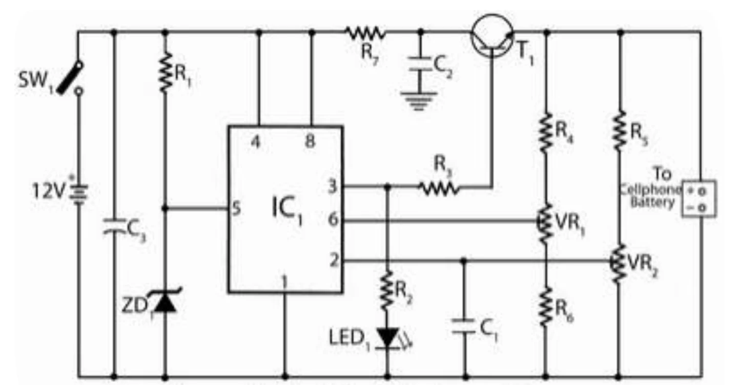
  The main part of the circuit mobile cellphone charger is timer IC NE555, used to charge and monitor the voltage level. IC1 get control voltage to pin 5 by zener diode ZD1­. Threshold pin 6 and trigger pin 2 is supplied with a voltage set by VR1 and VR2 respectively. The trigger pin 2 of IC1 is below 1/3VCC when discharge battery is connected to the circuit as a result flip-flop of IC1 is switched on to take output pin 3 high. The process is reversed when battery is fully charged of charged battery is connected. Here transistor T1 used to enhance the charging current from output pin 3 of IC1. Adjust potentiometer VR1 and VR2 as per require.

Parts List

Resistors (all ¼-watt, ± 5% Carbon)

R1 = 390 Ω

R2 = 680 Ω

R3 = 39 Ω/1W

R4 = 27 KΩ

R5 = 47 KΩ

R6 = 3.3 KΩ

R7 = 100 Ω/1W

VR1, VR2 = 20 KΩ

Capacitors

C1 = 0.001 µF (ceramic disc)

C2 = 0.01 µF (ceramic disc)

C3 = 4.7 µF/25V (Electrolytic )

Semiconductors

IC1 = NE555 timer IC

T1 = SL100 or any Medium power general purpose NPN transistor like: 2N4922 , 2N4921,2N4238, FCX1053A

ZD1 = 5.6 V/1W

LED1

Miscellaneous

SW1 = On/off switch

1.5V*8 AA cells

Mobile connector

Can I connect 12V 100Ah and 12V 200Ah batteries in parallel for a 12V system?

Can I connect 12V 100Ah and 12V 200Ah batteries in parallel for a 12V system?

People who don’t know about this topic are making totally incorrect recommendations. Yes, you certainly can, with no problem assuming you are talking about 2 batteries of the same type, i.e, lead-acid. As a percentage of their capacities, they will both charge and discharge at the same rate, though the current into and out of the 200Ah battery will always be about double that of the other. You cannot connect them in series at all, but you certainly can parallel them.I build battery park for inverter several times. I know a thing or two about batteries. This is absolutely the correct response and one you can bet your life on. End result is a 300Ah battery.
Do make sure to fully top-charge both independently before connecting together to avoid a huge spark. Then make connection of new battery to system through a low-value high-wattage resistance, something like 10 ohms, 10W. An incandescent light bulb will do as the resistor. Then once both batteries are at the same voltage/no voltage across the resistor, remove it and direct connect.
EDIT: For those who disagree with my answer, let me draw a parallel that is a near-perfect model. You have 2 large elevated rectangular water tanks which are at the same height and have equal height, but one’s cross-section is 1m x 1m while the other is 1m x 2m. Both are open at the top to the atmosphere. Directly under their bottoms is a pipe T-fitting connection connecting them, then a single pipe down to a valve and a load, let’s say a water turbine. The water pressure at the turbine is equivalent to the voltage of two subject batteries, the water in them is equivalent to the amp-hour capacity of each, and any flow of water out the bottom is equivalent to current going to a load. Now open the valve and let the turbine run. If you know anything at all about the physics of this, you already know that the water level in both tanks will be equal to each other by virtue of the T-fitting, and that as water drains from the two tanks, will remain level, even as the levels drop. There will never be a case where water drains from one tank into the other, and there will never be a case where the larger tank is not draining water at exactly double the rate of the smaller.
EDIT2, 5/13/2022 - Both AGM, 2.9Ah general purpose (partially charged), 8.5Ahr deep cycle/high power (fully charged), will comment later, but even if ratio of current into and out of not always precisely 2.93, still current is always approximately proportional to capacity. Both will converge more precisely once both fully recharged.